EN
EN
 AR
AR
 BG
BG
 HR
HR
 CS
CS
 DA
DA
 NL
NL
 FI
FI
 FR
FR
 DE
DE
 EL
EL
 HI
HI
 IT
IT
 JA
JA
 KO
KO
 NO
NO
 PL
PL
 PT
PT
 RO
RO
 RU
RU
 ES
ES
 SV
SV
 CA
CA
 TL
TL
 IW
IW
 ID
ID
 SR
SR
 SK
SK
 UK
UK
 VI
VI
 HU
HU
 TH
TH
 TR
TR
 FA
FA
 AF
AF
 MS
MS
 GA
GA
 HY
HY
 BN
BN
 MN
MN

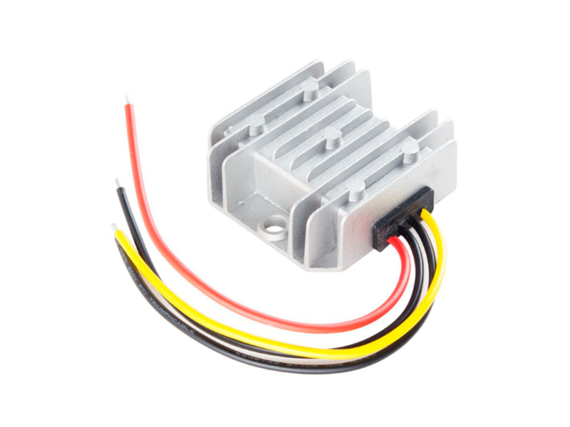
A buck-boost (feszültségcsökkentő-növelő) átalakító gyakori problémái és megoldásai
Ha elektronikai mérnök, aki olyan áramkörökkel dolgozik, amelyek meghatározott feszültséget igényelnek, valószínűleg már találkozott egy úgynevezett Buck-Boost átalakítóval. Ezek az eszközök rendkívül hasznosak, mivel képesek a feszültségek szabályozására és módosítására – növelésére vagy csökkentésére –, és gyakran használják őket mind mobil készülékektől kezdve egészen nagyobb ipari berendezésekig. Ugyanakkor néha nehézségeket okozhatnak, és meglehetősen sok türelmet igényelhet a megbízható működés elérése. Ez a cikk a gyakorlatban felmerülő leggyakoribb kérdésekre épít, beleértve tápegység-szakértők tapasztalatait is.
Melyek tehát a mérnökök által gyakran tapasztalt leggyakoribb problémák ezekkel az eszközökkel, és hogyan lehet őket megoldani? A részleteket gyakorlati, munkaasztal-központú szemszögből tárgyaljuk.
Az hatékonysági rejtély: Amikor az átalakító veszít energiát
Az egyik első és leggyakoribb probléma a Buck Boost átalakítók esetében az alacsony hatásfok. Egy energiaérzékeny alkalmazásokra szánt tervezés akkor alulműködhet, ha túl sok bemeneti teljesítmény disszipálódik ahelyett, hogy a terhelésre kerülne. Ez az elvesztegetett energia főként hővé alakul, ami túlmelegedést okozhat, és veszélyeztetheti a rendszer működését. Nagy kapcsolási veszteségek léphetnek fel, ha az áramkör MOSFET tranzisztorai túl lassan kapcsolnak ki vagy be, illetve ha nagy a kapcsolási zaj. Hasonlóképpen, ha olyan induktivitást használunk, amelynek magas a DC-ellenállása (DCR) vagy gyenge a maganyaga, akkor a komponensen belül jelentős mennyiségű energia hőként vész el. Emellett az aszinkron kialakítású áramkörökben a dióda – különösen nagy áramok mellett – szintén jelentős veszteségforrás lehet. A megoldás nem egy csodakomponens megtalálásában rejlik; hanem a gondos optimalizálásban. Fontolja meg egy fejlettebb kapcsolási algoritmussal rendelkező vezérlő használatát, alacsonyabb kapacitású és kisebb bekapcsolt ellenállású MOSFET-ek kiválasztását, valamint magasabb teljesítményű induktivitások alkalmazását.
Az optimális teljesítmény elérése érdekében számos teljesítményelektronikai gyártó szinkron tervezési megoldásokat alkalmaz, amelyek a veszteséges diódát egy másodlagos MOSFET-tranzisztorral helyettesítik. Az ilyen magas hatásfokú topológiára való áttérés jelentős teljesítménynövekedést és hatékonyabb energiafelhasználást eredményezhet.
Hűvösen maradni, amikor az átalakító felmelegszik
Szorosan összefügg az energiahatékonysági problémákkal a hőkezelés kihívása. Egy túlmelegedett Buck Boost átalakító majdnem minden alkatrészét károsíthatja – beleértve a vezérlő IC-t, MOSFET-eket, tekercset és kondenzátorokat is –, amely veszélyezteti az egész rendszer működését. A túlzott hő növeli a korai meghibásodás kockázatát, és csökkenti az általános megbízhatóságot. Ezek a hőproblémák általában elektromos veszteségekből származnak, amelyeket elégtelen hűtés vagy gyenge hőelvezetési utak súlyosbítanak. A nyomtatott áramkör (PCB) elrendezése itt különösen fontos szerepet játszik: ha a forró alkatrészeket, például a tekercset és a MOSFET-eket sarokba zsúfolják, elegendő rézfelület nélkül a hőelvezetéshez, helyi hőfókuszok alakulhatnak ki. Ezeknek a problémáknak a kezeléséhez kétrétű megközelítés szükséges: először is csökkenteni kell a hőtermelést az előbb említett hatékonyság-növelő intézkedések alkalmazásával; másodszor pedig javítani kell a hőelvezetést gondosan megtervezett PCB-kialakítással. Ez magában foglalja megfelelő méretű réz síkok használatát a teljesítményalkatrészek hőelvezető padjaihoz csatlakoztatva, hővezető átmenetek (vias) hozzáadását, valamint a megfelelő levegőáramlás biztosítását a ház belsejében.
Nagy teljesítményű terveknél ne habozzon kis hűtőbordát beépíteni. A professzionális DC-DC modulgyártók megértik, hogy az hatékony hőkezelés szerves része a tervezésnek – egy hűvös átalakító megbízható átalakító.
Stabilitás és zaj: A tiszta és stabil energia utáni kutatás
Az egyik legfrusztrálóbb probléma a rendszer instabilitásának és elektromos zajának diagnosztizálása. Ez véletlenszerű kimeneti feszültség-oszcillációkban, váratlan csengésben vagy más érzékeny analóg vagy RF áramköröket zavaró nagyfrekvenciás zajban nyilvánulhat meg ugyanazon a nyomtatott áramkörön. Ezek a problémák gyakran a szabályozóhurkból és a fizikai elrendezésből származnak. Egy rosszul kompenzált visszacsatolási hálózat bizonyos terhelési körülmények között instabillá teheti a rendszert, ami feszültségcsengést vagy oszcillációt eredményez. Hasonlóképpen, a hosszú vagy rosszul vezetett nagyáramú vezetékek parazita hatásokat idézhetnek elő, amelyek elektromágneses zavart (EMI) generálnak. A földelési sík tervezése is kulcsfontosságú szerepet játszik; ha nem megfelelően készül, zajvezetővé válhat. A részletekre való odafigyelés alapvető fontosságú. Mindig tartsa be a gyártó utasításait a visszacsatolási hurok stabilizálásához, és használja az ajánlott ellenállás- és kondenzátorértékeket. Az elrendezés tekintetében ajánlott gyakorlat a nagyáramú hurkok minél rövidebbre tervezése, illetve az egymáshoz kapcsolódó alkatrészek sűrű csoportosítása a paraziták minimalizálása és az EMI csökkentése érdekében. Ugyancsak alapvető fontosságú a megfelelő tömegkondenzátor és nagyfrekvenciás kondenzátorok kiválasztása, hogy biztosítsa a fejlett alkalmazások által igényelt tiszta, stabil tápfeszültséget.
Rendszerterv és megvalósítás kihívásai
A tipikus áramkörtervezési kérdések túlmutatva, egy Buck Boost átalakító sikeres megvalósítása gyakran a gyakorlati szempontoktól függ, mint például az alkatrészek kiválasztása és a valós működési körülmények. Az alkatrészek kizárólag adatlap szerinti specifikációk alapján történő kiválasztása váratlan problémákhoz vezethet. Például egy tekercs rendelkezhet a helyes induktivitásértékkel, mégis telítődhet az áramkör csúcsáramánál, ami éles hatásfok-csökkenést és az áramkörzaj hirtelen növekedését eredményezi. Hasonlóképpen az elektrolit kondenzátorok felmelegedhetnek, és teljesítményük romolhat a konverter hőkörnyezete miatt. Továbbá olyan tervek, amelyek tökéletesen működnek a laborban, a mezőn meghibásodhatnak környezeti tényezők miatt, mint például hirtelen hőmérsékletváltozások vagy rezgés. A megoldás a tartalékkal történő tervezés: alkatrészek leterhelése és a valós világbeli terhelések előre figyelembevétele. Válasszon olyan tekercset, amelynek telítődési áramértéke legalább 20–30%-kal magasabb a számított csúcsáramnál. Alacsony ESR-jű, minőségi kerámia kondenzátorokat használjon csatolásra, és fontolja meg erős polimer vagy tantál kondenzátorok alkalmazását nagyobb szűrésekhez magas hőmérsékletű környezetben. Végül mindig tesztelje a prototípusokat a teljes működési hőmérséklet-tartományon keresztül és különböző terhelési feltételek mellett.
Ez a részletes érvényesítési folyamat különbözteti meg a működő prototípust a teljesen robosztus, gyártásra kész terméktől, amely megbízható teljesítményt nyújt szerteágazó alkalmazásokban. A robusztus tervezésre és alapos tesztelésre helyezett hangsúly révén a mérnökök biztosíthatják, hogy az áramátalakító rendszerek folyamatos és megbízható teljesítményt nyújtsanak.
Ajánlott termékek
Aktuális hírek
-
A nem izolált BUCK konverterek alkalmazási előnyei az izolált léptető konverterekhez képest
2024-01-23
-
A DC-DC konverterek kiváló előnyökkel rendelkeznek a külső hálószabadságú alkalmazásokban
2024-01-23
-
DC to DC akkumulátor töltő – Széles bemeneti tartomány és zajellenálló képesség dual akkumulátorszisztémák alkalmazásához
2024-01-19